Posts tagged retro
Shocking Finale
30 October 2023 (programming retrochallenge retrochallenge2023 retro homelab)Sunday, 15th October. Day of the HomeLab-2 game jam deadline. My port of The Revenge, or at least its first half, is fully playable. It even has quicksaving/loading implemented, with an in-memory buffer. Unfortunately, I didn't have time to find out what it would entail to implement persistent saving on cassette, but at least with quicksaving you can play cautiously enough to avoid frustrating deaths.
But can you actually win the game? To make sure you can, I wanted to play through from start to finish, using the hacked-up game scripts I ended up with that has a lot of the locations and scripts stripped. I could have just played the whole thing on a HomeLab-2 emulator, but I wanted something a bit more streamlined for two reasons:
- Because of the horrible foil keyboard of the real HomeLab-2, the firmware's keyboard sensing is a bit flakey when emulated on modern hardware with precise keypress detection, and so it's common to end up with unwanted key repetitions.
- If it turns out there's some flaw in the game scripts somewhere in the middle, I didn't want to replay the whole game from scratch after fixing the bug, reassembling and then reloading it into the emulator.
There and Back Again
27 October 2023 (programming retrochallenge retrochallenge2023 retro homelab)So here we are, with a couple days to go until the deadline, with a text adventure game that is roughly 22 KB in size, targeting a machine with 16 KB of RAM.
One thing to try would be to start trimming content. This is a straightforward idea: if we can remove messages and pieces of the script, then the size goes down. We know that the "empty" game (i.e. just the engine plus its runtime memory usage) is 2 KB, so by the intermediate value theorem, if we remove enough content, the size at some point will get below 16 KB.
But removing content from a text adventure game is not as easy as it might first sound, if you only have a couple days remaining to do that plus finish the engine plus do enough testing to make sure the game can still be finished. The reason for that is that most of the rooms, almost all objects, and most possible interactions are all there as part of some puzzle, with the whole game's start and end connected through a chain of the puzzles. Remove something and you might break a link and make the game unplayable. Perhaps even worse is if technically it doesn't become unplayable, but you remove something that contains the crucial information that would prompt the player to come up with a solution, and thus instead of a puzzle, now you have a "guess the random input you need to type in" game.
The other way to make the game smaller is to cut it in half: take some mid-point event, and turn that into the winning condition. This should allow you to remove all the rooms that are normally available only after that mid-point event; then, you can remove the scripts that are keyed to the removed rooms; and then you can remove the messages that are not referenced by the remaining scripts anymore.
To pull this off, you need a good middle point that makes sense as the new game not just technically, but narratively as well. Luckily, I've found such a point in The Revenge. So the original game's plot (spoiler alert for a 35-year-old Hungarian text adventure game!) is that random Japanese rural dude is sent to fetch water, arrives back to find his village razed and burned by some evil local warlord, and swears revenge (TITLE DROP!). Goes to the city, finds the warlord's mansion, but surprise surprise, it's heavily guarded. So after some local adventuring the protagonist ends up on a ship to China, living in a monastery for a while acquiring stamina through rigorous exercise, then learns kung-fu from an old master whose daughter he saves from bandits. Armed with deadly fists, he returns to Japan on a perilious trek through shark-infested waters on a dinghy, infiltrates the mansion and finally confronts the evil warlord. Standard kung-fu B movie plot.
On the one hand, the good news is that there is a very natural way to split this into two episodes: the first episode can end with the protagonist learning kung-fu, leaving the actual confrontation with the Big Bad to the second episode. On the other hand, as you can see from this structure, you don't actually get to remove half the locations by just keeping half the game, because the second half mostly consists of coming back to Japan and revisiting the same places, just now with the ability to defeat opponents in hand-to-hand combat.
On the gripping hand, we don't need to cut down our memory usage by half -- we just need to reduce it by 6 KB, or 30% of our original 20 KB asset size. That should be doable.
For the technical details, the idea is the following. First of all, let's briefly look at what the game script looks like. Here's some example bytecode that scripts a single interactive response.
1d            Length of second room's scripts, for easy indexing

10            Length of next script, for easy skipping if the input doesn't match
3a 78 00      Matches user input consisting of word 3a "fill" and 78 "bucket"
08 78 02      If item 78 is not here (in inventory or in current room), print message 2 and end
06 0a 29      If variable 0a is not 0, print message 29 and end
04 0a         Set variable 0a to ff
02 04         Print message 4
14 0b         Play chime 0b
00            End

05            Length
33 a4 00      Input: 33 "swim" a4 "river"
0c 03         Go to location 03 "island"

04            Length
02 00         Input: 02 "northeast"
0c 04         Go to location 04 "hillside above village"

00            End of handlers for room 2

15            Length of room 3's handlers
...           Room 3's script
(I should note here that since my HomeLab-2 version has no "multimedia", all bytecode operations like show picture P or play chime C are stripped during conversion.)
Now let's suppose we wanted the game to end in this room without the ability to progress to the island. We can remove the second handler in its entirety (saving 6 bytes in the process), and then statically re-traverse the remaining bytes to find all go to location X commands. When viewing the result as a directed graph, we will see that room 03 is no longer reachable from the starting location, and so we can throw away the script in the next 22 (including the length) bytes. Then we can build similar accessibility information from the remaining bytecode, this time not for the rooms, but for the messages. For example, message 29 is definitely needed (since it is referenced in room 2), but there might be other messages that are only referenced in the 22 bytes we've just thrown away.
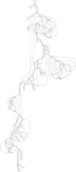
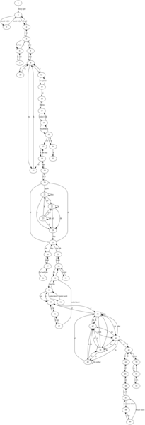
By the way, for some eye candy, here's what the map looks like. The left-hand side shows the original map. Rooms 8 to 13 and 70 to 76 comprise two of those super annoying mazes that old text adventure games were keen to include. The right-hand side shows the map of The Revenge Episode 1, i.e. my cut-in-half HomeLab-2 version. Simplifying the episode one maze didn't really save much space since all the constituent rooms use the same text descriptions, but I think skipping them simply makes the game better.
Of course, there are also location-agnostic interaction scripts involving carriable items; since with the changes to the map, I already fit into memory (if just barely), and time was quickly running out, I decided not to bother pruning the scripting of items that are not aquirable in the first half of the game.
So I had a fully playable game with even enough space left to implement a simple in-memory gamestate saving facility, which is useful because there are quite some lethal situations in the game. At this point I had one day (a Sunday) remaining, and I thought it was going to be smooth sailing: my plan was to play through the modified script in a desktop interpreter (with replaying and checkpointing capabilities) to make sure the game is winnable, convert it to a WAV file for deployment, and send it in.
Join me in the next post to read why that last day was anything BUT smooth sailing. DUN DUN DUUUUUUUUUUN!

An Idea for a Grand Adventure
24 October 2023 (programming retrochallenge retrochallenge2023 retro c64 homelab)Two weeks before the game jam deadline, I finally had the idea for my main entry. But with most of the first week occupied with work and travel, will the second week be enough to make it a reality?
Years ago, after remaking Time Explorer, I went on to reverse-engineer István Rátkai's subsequent games for the Commodore 64: The Revenge, and New Frontier I and II. This work culminated in a crowd-funded modern Android release. These Android versions were possible because these text adventure games, in quite forward-looking way for 1988, were originally written in a small homebrew bytecode language that was then packaged up with an interpreter. Think of it like a very primitive version of Infocom's Z-machine, but without all the Lisp-y sensitivities.
So anyway, my idea was to take the game's scripts as-is, and implement my own bytecode interpreter for the HomeLab-2. The Commodore 64 has 64 KB of RAM, while the HomeLab only has 16; but surely if I get rid of the multimedia (the per-room graphics and the small handful of short melodies played at key points of the games), the remaining text and scripts can't be that much?
Well it turns out when talking about text adventure games for 8-bit home computers, all that text is actually relatively quite a lot! In The Revenge, for example, just the various messages printed throughout the game fill 16 KB, and then we have 10 more KB of the recognized words and the game script. Clearly, this 26 KB of data will not fit into 16 KB, especially not leaving enough space for the game engine itself and the 256 bytes of game state.
Well, what if we try to be a bit more clever about representation? For example, because of the HomeLab-2's fixed upper-case character set, all that text will be in upper-case and without using any Hungarian accented characters, so we can use something similar to ZSCII to store 3 characters in 2 bytes. This, and some other small tricks like encoding most message-printing in just a single byte instead of a byte to signal that this is message-printing followed by the byte of the message ID, gets us to below 20 KB. Still not good, but better!
It was at this point that I also started writing the engine, to see how big that will be. Of course, at this point I was only able to try it out by only including a subset of the rooms and the game script, but at least it allowed me to get a size estimate for it. And so it came to about 1.5 KB of code to implement everything, plus 256 bytes of game state. Optionally, if we have space left, we can use a second 256 bytes to implement quicksave/quickload.
So what will we do with our budget of 14 KB, given a 20 KB game? Let's find out in the next post.
Getting my HomeLab-2 sea legs
21 October 2023 (homelab programming retrochallenge retrochallenge2023 retro haskell)Previously, we left off our HomeLab-2 game jam story with two somewhat working emulators, and a creeping realization that we still haven't written a single line of code.
Actually, it was a bit worse than that. My initial "plan" was to "participate in the HomeLab-2 game jam", with nothing about pesky details such as:
- What game do I want to make?
- What technology will I use?
- How will I find time to do it, given that I'm spending all of September back home in Hungary?
I found the answers to these questions in reverse order. First of all, since for three of the five weeks I've spent in Hungary, I was working from home instead of being on leave, we didn't really have much planned for those days so the afternoons were mostly free.
Because the HomeLab-2 is so weak in its processing power (what with its Z80 only doing useful work in less than 20% of the time if you want to have video output), and also because I have never ever done any assembly programming, I decided now or never: I will go full assembly. Perhaps unsurprisingly, perhaps as a parody of myself, I found a way to use Haskell as my Z80 assembler of choice.
This left me with the question of what game to do. Coming up with a completely original concept was out of the quesiton simply because I lack both the game designing experience as well as ideas. Also, if there's one thing I've learnt from the Haskell Tiny Games Jam, it is that it's better to crank out multiple poor quality entries (and improve in the process) than it is to aim for the stars (a.k.a. that pottery class story that is hard to find an authoritative origin for). Another constraint was that neither of my emulators supported raster graphics, and I was worried that even if they did, it would be too slow on real hardware; so I wanted to come up with games that would work well with character graphics.
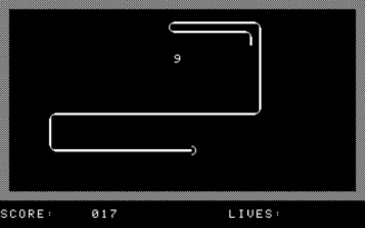
After a half-hearted attempt at Tetris (which I stopped working on when someone else has already submitted a Tetris implementation), the first game I actually finished was Snake. For testing, I just hacked my emulator so that on boot, it loads the game to its fixed stating address, then used CALL from HomeLab BASIC to start it. This was much more convenient than loading from WAV files; doubly so because it took me a while to figure out how exactly to generate a valid WAV file. For the release version, I ended up going via an HTP file (a byte-level representation of the cassette tape contents) which is used by some of the pre-existing emulators. There's an HTP to WAV converter completing the pipeline.
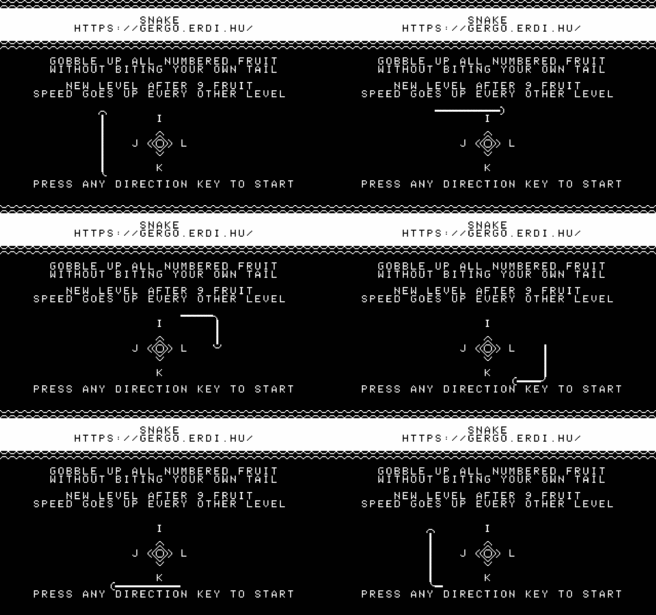
There's not much to say my Snake. I tried to give it a bit of an arcade machine flair, with an animated attract screen and some simple screen transitions between levels. One of the latter was inspired by Wolfenstein 3D's death transition effect: since the textual video mode has 40×25 characters, a 10-bit maximal LFSR can be used as a computationally cheap way of replacing every character in a seemingly random (yet full-screen-covering) way.
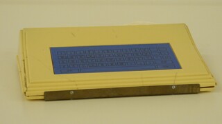
For my second entry, I went with 2048. Shortly after finishing Snake, thanks to Gábor Képes I had the opportunity to try a real HomeLab-2 machine. Feeling how unresponsive the original keyboard is convinced me that real-time games are not the way to go.
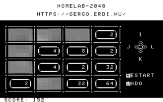
The challenge with a 2048-like game on a platform like this is that you have to update a large portion of the screen as the tiles slide around. Having an assembler that is an EDSL made it a breeze to try various speedcoding techniques, but with lots of tiles sliding around, I just couldn't get it to fit within the frame budget, which led to annoying flickering as a half-finished frame would get redrawn before the video refreshing interrupt handler eventually returned to finish the rest of the frame. So I ended up using double buffering, which technically makes each frame longer to draw, but avoids inconsistent visible frames.
Since the original 2048 is a product of modern times, I decided to pair my implementation with a more clean design: just like a phone app, it boots straight into the game with no intro screen, with all controls shown right on the main screen.
Between these two games, and all the other fun stuff one doesn when visiting home for a month, September flew by. As October approached, I stumbled upon this year's RetroChallenge announcement and realized the potential for synergy between doing something cool in a last hurrah before the HomeLab-2 game jam deadline and also blogging about it for RetroChallenge. But this meant less than two weeks to produce a magnum opus. Which is why this blogpost series became retrospective — there was no way to finish my third game on time while also writing about it.
But what even was that third and final game idea? Let's find out in the next post.
So... HomeLab-2? What is that?
18 October 2023 (homelab programming retrochallenge retrochallenge2023 retro javascript idris)I don't blame you if you don't know what a HomeLab-2 is. Up until I listened to this podcast episode, I didn't either. And there's not much info online in English since it never made it out of Hungary.
As interesting as the history of this "Soviet bloc Homebrew Computer Club" machine is, I will be skipping that here and concentrate on the technical aspects.
Basic architecture
HomeLab-2 is a home computer in the eighties sense: a computer that boots to a BASIC interpreter, with a built-in keyboard, video output that can be connected to a TV.
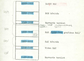
The core of the machine is the well-known Zilog Z80 CPU, one of the stars of this class of computers (the other one being, of course, the MOS 6502). It is connected to 8 KB of ROM containing the BASIC interpreter, some IO routines for thing like loading programs from cassettes, and a rudimentary monitor. The system also comes with 16 KB of general purpose RAM (upgradeable to 32 KB), and 1 KB of text-mode video RAM coupled with a 2 KB character set ROM that is inaccessible to the CPU.
One interesting aspect of the machine is that due to export restrictions and a weak currency, availability of more specialised ICs was limited, and so the HomeLab-2 was designed around this limitation by only using 7400-series ICs beside the Z80. This meant that a lot of the functionality that you would expect to be done with custom circuitry, chief among them the video signal generation, was done by the CPU bit-banging the appropriate IO lines. This is somewhat similar to the ZX80/81 video generator, in that the CPU "jumps" to video memory so that its program counter can be used as the fastest-possible-updating software counter, and the supporting circuitry makes sure the CPU's data lines are fed NOPs. Concretely, the value appearing on the data bus is 0x3F, which is effectively a NOP (it inverts the carry flag) and makes it easy to conditionally change it to a 0xFF, i.e. a RST 38, which is used to mark end-of-(visible)-line.
To program the HomeLab-2, you don't need to know the exact details of this, but it is important to keep in mind that as long as the video system is turned on, the CPU will spend 80+% of its time drawing the screen, leaving your program with less than 20% of its 4 MHz speed.
Data storage is done to cassette tape, via an audio mic/speaker port. Writing to a specific memory location sets the audio output into its high level for about 10 μs. The on-tape format is based on simple 10 μs-wide square waves 1.6 ms apart: for high bits, this interval is halved by an extra mid-point square. Of course, for the CPU to be able to accurately keep track of the audio signal timing, the video system has to be turned off while accessing the tape.
The audio output is also routed to an internal speaker so you can generate sound by modulating this 10 μs square.
The emulation sitch
To get started with HomeLab-2 development, we need some way of testing programs. A straightforward tool of doing that is an emulator of the machine. Unfortunately, at least back in August when I started working on my games, the emulator situation wasn't quite rosy.
The obvious place to check first is MAME, and indeed it claims to support the HomeLab-2. However, it was obviously written as a quick hack by someone who didn't really invest the time into understanding how the original machine's video system worked. This of course wreaks havoc with the timings, and makes it impossible to get cassette IO working.
Discounting very old emulators running on DOS, the other one I found was Attila Grósz's emulator of the whole HomeLab family, which had an update as recently as May 2022, but its HomeLab-2 support was quite limited. And much more annoyingly, it's a Windows-only closed source software. I don't want to dunk on the guy, but that's just stupid; especially because looking at the source of actual working emulators is usually a really good way in resolving any ambiguities in documentation during development. And realistically, what benefit can you possibly hope from your closed-source emulator of a computer that in our Lord's year of 2023 probably interests about a dozen people?!
So I did what any responsible adult would do when faced with a limited-time game jam where he has to also learn Z80 assembly and figure out, well, everything: I set out to put all that aside and cobble together my own emulator. With blackjack and hookers, of course.

My first emulator
Oops I guess the section title is a spoiler.
I wanted to make something that people can just use without any fuss, so I decided to target web browsers and make it into a single-page app. The goal was to quickly get something off the ground, publish it so that others can also use it for the game jam, and then later hope for contributions from people who know the machine better.
Because I was in peak "just get the damn thing working" mode, I decided to write vanilla JavaScript instead of transpiling from some statically typed functional language, which is what I would normally do. With JavaScript, at least I knew that whatever happens, the code might end up as a horrible mess of spaghetti but at least I won't run into situations where I'm "the first guy to try doing that" and everything breaks, which is usually how it goes with these projects of mine.
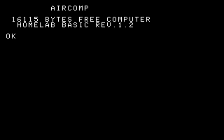
For the CPU core itself, I found an easy-to use Z80 emulator library. I connected it to some array-backed ROM and RAM, started rendering the text video RAM onto a canvas, and let the firmware rip. This got me all the way to the BASIC prompt, not bad for a couple minutes of hacking:
Getting from this to actually blinking the cursor and accepting input was much trickier, however. Remember all that detail a couple paragraphs ago about how the video system is implemented, what fake read values appear on the data bus as the video memory is scanned, that sort of stuff? That was not documented at all. The users' manual only mentions that the NMI "can't be used" for user purposes because it is used by the video system. I pieced the rest together mostly from reading the firmware disassembly, observing the CPU's behaviour, looking at the schematics, and doing a lot of "now if I were designing this machine, how would I do things?".
Eventually I got enough working that text-mode video worked; and then I gave up on raster video because I knew I wouldn't need it for the kinds of games I was envisioning. Then I added cassette IO, which necessitated a cassette player UI which then became way too much, and I kind of lost steam. But hey, at least I lost steam after I've got everything working. Well, everything except sound and raster graphics. But definitely everything that I was planning to use for my games!
This emulator, named HonLab (because HomeLab, and it runs on a web page, and honlap is Hungarian for home page, ha ha very clever, get it?! yeah sometimes I crack myself up!) can be used online here and its source code is on GitHub here.
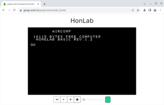
Now, at this point, the game jam deadline was rapidly approaching, and I still haven't written a single line of Z80 assembly, so it was time to finally...
Writing a second emulator
Oh my god what is wrong with me.
Also, this blogpost is starting to take too long to write, so long story short: based on my previous good experience with Idris 2's JavaScript backend and also itching to use Stefan Höck's new SPA FRP library, I decided to write a new version from scratch (only reusing the Z80 core), but this time in Idris 2. It's almost as finished as the first version, just missing the ability to save to tape; you can look at its source here and it was exactly the kind of project that I initially wanted to avoid: one where a significant amount of my time went into reporting upstream bugs and even fixing some. Time enjoyed wasting, and all that.
Also, because the two emulators do look the same from the outside, I won't bother making another screenshot; you wouldn't notice it anyway.

So by the next post, we'll finally get to the beginning of September, when I started writing Actual Lines of Code.
Older posts:
- 16 October 2023: Another year, another RetroChallenge
- 2 May 2022: Cheap and cheerful microcode compression
- 18 September 2021: Rust on the MOS 6502: Beyond Fibonacci
- 17 November 2020: A tiny computer for Tiny BASIC
- 30 September 2018: Composable CPU descriptions in CλaSH, and wrap-up of RetroChallenge 2018/09
- 23 September 2018: CPU modeling in CλaSH
- 22 September 2018: Back in the game!
- 15 September 2018: Very high-level simulation of a CλaSH CPU
- 8 September 2018: PS/2 keyboard interface in CλaSH
- 2 September 2018: CλaSH video: VGA signal generator
- 29 August 2018: RetroChallenge 2018: CHIP-8 in CλaSH
- 5 June 2015: Időrégész 2015
- 2 March 2015: Initial version of my Commodore PET
- 29 March 2014: My first computer
- 31 December 2013: Brainfuck on the Commodore 64

