My first computer
29 March 2014 (programming haskell fpga electronics retro chip-8)tl;dr: I've built a computer on a Xilinx FPGA using Kansas Lava, based on a virtual machine design from the mid seventies.
I would be lying if I said I always wanted to build my own computer. For a very long time, hardware didn't tickle my curiosity at all; and even today, I prefer staying away from dangling wires and soldering irons. I like my computing platforms to Just Work™, and hardware problems are just a huge hassle. But then in 2010 some coworkers of mine started getting into electronics and I learned from them just enough to start hooking some ICs up on a breadbord, and it seemed like a very fun diversion from all the high-level, abstract, softwarey stuff. In some sense, it filled the same void in me that assembly programing would probably have had. But even back in the days on the Commodore 64, I was looking for more BASIC extensions instead of going downwards to assembly / machine code.
One thing led to another and I was creating a Brainfuck CPU on a Papilio FPGA. It was a very satisfying experience, plus, I got to learn about a completely new world (that of digital hardware design and hardware description languages). So ever since then, I had a voice in the back of my head saying I should go all in, and implement a proper full computer, with I/O and all. But jumping straight into replicating a real computer seemed like trying to run before I can walk.
I can't remember now how I bumped into the CHIP-8 platform, but when I read about it in detail, I realized this is something I, a self-taught HDL guy, could realistically implement. To recap, it's a virtual machine spec from the mid seventies indended to be implemented on home computers of the time. It is super low performance, meaning I could implement everything the most naïve way possible and still get something workable out of it: graphics is 64×32 black & white, RAM is short of 4KBytes, CPU speed is not really part of the spec, and the only timers provided run at 60 Hz.
I can do this!
Setting the scene
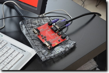
The FPGA board that I targeted is a Papilio One 500K, which has 500K... somethings called "system gates", and about 40KByte of SRAM. The Arcade MegaWing provides a D-sub 15 VGA connector and two PS/2 ports, among some other stuff that I am not using for this project.
The home computer targeted by the original CHIP-8 spec only had a four-by-four keypad, so I am not 100% happy about using a PS/2 keyboard for the input. Maybe a later version could use a bespoke keypad connected to the unused pins of the LogicStart MegaWing. However, by using a PS/2 keyboard, I could not worry about the hardware side of things and just implement a decoder for the PS/2 protocol.
In terms of software, there are several games available for the CHIP-8. Maybe even donzens! But just for fun, after finishing the machine itself, I ended up writing my own game as well: a crappy port of the currently trending 2048 game.
Understanding the CHIP-8
I would say the CPU itself is a RISC architecture, in that it has 16 registers and not a whole lot of operations. But I'm not sure it would be called RISC back in its day.
The aforementioned 64×32 one-bit graphics is manipulated via a sprite interface: there's a special CPU opcode for xor-blitting an 8-pixel-wide, variable-height sprite onto any part of the screen. I went with the obvious way of implementing it as a 2048-bit frame buffer.
To validate my understanding, I first created a software emulator in Haskell. That unearthed a ton of edge cases and situations where I was not reading the spec with enough attention. Once I had the emulator working well enough to play the sample games I found, I enumerated the modules I'll need to implement.

A TODO list
Since I've already done the Brainfuck CPU, I didn't foresee too much difficulty in implementing the CPU proper (oh boy was I wrong). However, the world of peripherals was a new one to me.
I've never looked into VGA signal timings in detail before, and for some reason I just assumed that it's going to be just as complicated as PAL, about which I knew just enough to know that you have to generate all kinds of elaborate sync patterns. So actually reading the VGA spec was a relief, and I quickly came up with a scheme where my CHIP-8 computer would be running at 50 MHz, so that it can easily implement the 25 MHz pixel clock needed for 640×480@60 Hz. I went with this mode because it has several advantages:
- It refreshes the screen at 60 Hz, so I can synchronize the CHIP-8 timers to it
- It has square pixel aspect ratio
- It is a "default" mode, so I can be confident that if I generate the correct signal, modern LCDs will be able to display it. In fact, for testing, I later got a 7" CCTV LCD with a VGA input on the cheap, so that I didn't have to make room for the 21" TFT I had lying around. The CCTV monitor supports three VGA video modes, and 640×480@60 Hz is one of them.
- By dividing both the horizontal and vertical resolution by 8, I can get 80×60 which doesn't leave too much unused border around 64×32. I could use all horizontal screen real estate if I divided by 10 instead, to get 64×48, but I have no idea how I could divide my horizontal/vertical position counter by 10; whereas dividing by 8 is a simple matter of shifting to the right by 3 bits.
The Papilio One itself has a clock of 32 MHz, and I first hoped that 32 Mhz and 25 Mhz is close enough that I can just generate a signal using the 32 MHz as the pixel clock. Turns out that's not quite how signal timings work.
Luckily, I've found out that the Papilio One also has something called a DCM which can divide and multiply the clock signal. I was able to go to 25 or 50 MHz easily with it. It's a bit of a black box component: I had to run a wizard in the Xilinx IDE to get a small binary file describing my DCM parameters, and then I integrated it into my build process by running another Xilinx program on it which spits out some magic bitstream.
The PS/2 protocol is a simple serial protocol with a slow (~10 KHz) clock and one parity bit per 8 data bits. Decoding it into a stream of bytes was a straightforward thing once I hunted down an actual PS/2 keyboard, since it turned out those USB to PS/2 dongles don't really work with regular USB keyboards; rather, the keyboard have to be made ready to "speak" PS/2 over the dongle. So I ended up getting a proper PS/2 keyboard from Mustafa Centre (thanks to Viki's sister Dori for picking it up for me); god only knows why they still had one on stock.
Tooling
The Xilinx tool suite seems to be aimed at being used from the IDE. This has several drawbacks: version controlling is complicated because generated artifacts litter the source tree; the editor itself in the IDE is of course crap compared to Emacs; and most importantly, I didn't intend to manually write either VHDL or Verilog. As I've mentioned before in my post about the Brainfuck CPU, I've found both of these hardware description languages to be lacking in the same way mainstream imperative programming languages are: the tools you, the developer, is given to introduce your own abstractions are very poor. So I planned to use Kansas Lava, an HDL embedded in Haskell.
Now, the first thing to note about Kansas Lava is, as nice at is, the software package itself is bit-rotten. The latest version available on Hackage cannot even be compiled with GHC 7.6. While the change to fix that is trivial, after that, you can easily bump into bugs in the Lava compiler itself. But more on that later. Later versions available from GitHub are not even self-consisent between the various dependencies. I've put my patched-up version of Kansas Lava and some of the packages it dependens on on GitHub and I'm trying to get Andy Gill to allow me to upload the bundle as a 0.2.4.1 update to Hackage. Don says I should maybe say fuck it and create my own Singapore Lava fork, just to stay with the Lava tradition of a twisty little maze of incompatible forks, all alike.
However, when it all works, it is amazing. I was able to extend the library of Papilio-specific Lava code that I created for the Brainfuck project with reusable modules for the VGA signal generator and the PS/2 decoder in such a way that they should be very easy to be re-used for any other future projects. And it's all type-safe, so for example, the Papilio Arcade MegaWing VGA port is statically enforced to be 4+4+4 bits whereas the LogicStart MegaWing is 3+3+2.
But there was one bug that left a bitter aftertaste in my mouth. Once I had both the CPU and the VGA parts working and I started running some test programs on the thing, I noticed that the framebuffer blitting is exhibiting "or" behaviour instead of "xor". Running the same code in the Lava simulator and dumping the contents of the framebuffer, it showed the correct, "xor" behaviour. After weeks of frustration and a complete rework of the communication system between the CPU, the VGA signal generator and the frame buffer to add memory read bussing, I finally took a look at the Lava compiler's source code to find that it simulates the xor2 primitive as xor but compiles it to or. How do you not notice this bug? Has the Kansas Lava suite been used by anyone for everything at all in the history of ever???
End result
The final result, after much trial and error, looking at the Lava simulator's output, and pouring over the code, is available here. I'm reasonably happy about the code base, except for the implementation of the CPU itself, which feels a bit spaghetti to me. Especially around the parts where it's waiting for results to come back from main RAM or the video framebuffer.
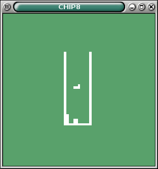
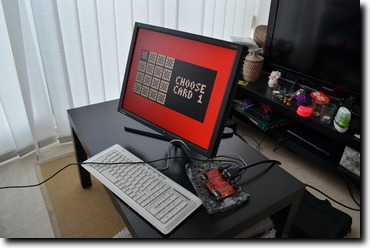
Below are some photographs and videos of it running two games: the memory puzzle game Hidden and the 2048 clone mentioned above. Unfortunately, the Tetris game from the screenshot above seems to have a bug in its input handling, in that it samples the keyboard at an unthrottled frequency; thus, even the shortest keypress sends the falling piece to the edge of the wall. I'll eventually need to disassemble the game and fix this.
The VGA signal generator is not as neat as it could be, because it doesn't do pre-fetching. This means by the time the current CHIP-8 pixel's value is read from the framebuffer, it is already too late, the first of the 8 real pixels for the given virtual CHIP-8 pixel should already have been drawn. This results in some ghosting. But since I know what's causing it, I will hopefully be able to fix this in some next version. But right now I'm too happy to have the whole thing just working.


